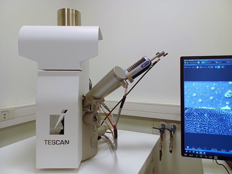
The department has a Tescan VEGA scanning electron microscope (SEM) capable of imaging very small objects and simultanously quantifying the element content.
SEM can be used for research and educational purposes within a range of disciplines such as geoscience, archaeology, bioscience, material science, engineering and chemistry, where you want to e.g. investigate particle morphology (particle size, shape, structure etc.) and characterize minerals, metals, rocks, hydrocarbons, microfossils and other materials in situ.
This scanning electron microscope can perform different types of analyses, e.g. points, line-scans or mapping. The specimens can be single particles or material mounted on stubs, thin sections or polished blocks.
Technical facts:
Depending on the material it is recommended to coat the specimens with e.g. carbon, platinum or gold.


